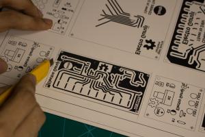
Mastering Printed Circuit Board Design: A Comprehensive Guide

-
Quick Links:
- Introduction
- Understanding Printed Circuit Boards
- Types of Printed Circuit Boards
- Materials and Tools Needed
- Designing Your PCB
- Printing Techniques
- The Etching Process
- Assembly and Testing
- Common Issues and Troubleshooting
- Case Studies
- Expert Insights
- FAQs
Introduction
Printed Circuit Boards (PCBs) are the backbone of modern electronics. From smartphones to home appliances, they are essential in connecting electronic components. This guide will walk you through the entire process of creating a PCB, from design to testing, ensuring you have all the knowledge to produce your own circuit boards.
Understanding Printed Circuit Boards
A printed circuit board is a thin board made of insulating material, with conductive pathways etched onto its surface. These pathways connect various electronic components, allowing them to communicate effectively.
- Functionality: PCBs serve as the foundation for electrical circuits.
- Design: They can be single-sided, double-sided, or multi-layered.
- Applications: Used in consumer electronics, automotive, aerospace, and medical devices.
Types of Printed Circuit Boards
Understanding the different types of PCBs is crucial for selecting the right one for your project:
- Single-Sided PCBs: These have only one layer of conductive material and are the simplest form.
- Double-Sided PCBs: These allow for connections on both sides, increasing complexity and functionality.
- Multi-layer PCBs: Composed of multiple layers of material, ideal for complex circuits.
Materials and Tools Needed
Creating a PCB requires specific materials and tools. Here’s what you’ll need:
- Materials:
- FR-4 or CEM-1 board
- Copper foil
- Silkscreen ink
- Photoresist or etching solution
- Tools:
- PCB design software (e.g., Eagle, Altium Designer)
- Laser printer or photoplotter
- Etching tank
- Drill press
Designing Your PCB
The design phase is critical in PCB creation. Follow these steps to create your design:
- Define the Circuit: Start by sketching your circuit diagram using software.
- Lay Out the PCB: Arrange components logically to minimize traces and optimize space.
- Route Traces: Connect components with traces, ensuring proper width and spacing.
- Finalize Design: Review the design for errors, ensuring all connections are made.
Printing Techniques
Once your design is ready, it’s time to print it onto the PCB material. Here are popular techniques:
- Laser Printing: Produces high-resolution prints suitable for photoresist.
- Screen Printing: Ideal for creating silkscreen layers for component labeling.
The Etching Process
Etching is crucial for transferring the printed design onto the PCB material. Here’s a step-by-step guide:
- Prepare the Board: Clean the board thoroughly to remove any contaminants.
- Apply Photoresist: Coat the board with photoresist for UV exposure.
- Expose to UV: Use a UV light to expose the board, hardening the photoresist where needed.
- Develop the Board: Rinse the board in a developer solution to remove unexposed photoresist.
- Etch: Place the board in an etching solution to remove unwanted copper.
Assembly and Testing
Now that you have your etched PCB, it’s time to assemble the components:
- Component Placement: Position all components according to your design.
- Soldering: Use soldering techniques to secure components in place.
- Testing: Conduct tests to ensure functionality, checking for shorts and open circuits.
Common Issues and Troubleshooting
Creating PCBs can come with challenges. Here are some common issues and how to fix them:
- Short Circuits: Check for solder bridges and correct any errors.
- Open Circuits: Verify connections and trace continuity with a multimeter.
- Component Placement Errors: Double-check your layout against the design.
Case Studies
Here are a few case studies of successful PCB projects:
- Project A: A small startup developed a custom PCB for a wearable device, reducing production costs by 20%.
- Project B: An educational institution created a PCB for a robotics competition, enhancing student engagement and learning.
Expert Insights
We spoke to industry experts to gather insights on PCB design:
"Focus on design simplicity. The fewer components, the easier the assembly and testing." - John Doe, PCB Design Expert
"Invest in quality materials. They can significantly impact the durability and functionality of the PCB." - Jane Smith, Electronics Engineer
FAQs
- What is a printed circuit board?
A printed circuit board is a flat board that connects electronic components using conductive pathways.
- What materials are used in PCB manufacturing?
Common materials include FR-4, copper foil, and various insulating substrates.
- How do I design my PCB?
Use PCB design software to create a schematic, layout components, and route traces.
- What are the different types of PCBs?
Single-sided, double-sided, and multi-layer PCBs are the most common types.
- Can I create PCBs at home?
Yes, with the right materials and tools, you can create PCBs at home.
- How long does it take to create a PCB?
The time varies, but creating a basic PCB can take a few hours to days depending on complexity.
- What are common issues faced in PCB manufacturing?
Common issues include short circuits, open circuits, and misaligned components.
- How do I test my PCB?
Use a multimeter to check for continuity and ensure all connections are functioning.
- What software can I use for PCB design?
Popular options include Eagle, Altium Designer, and KiCAD.
- Is professional PCB manufacturing expensive?
Costs depend on complexity, size, and quantity, but can be affordable for small batches.
Random Reads
- Mastering the art of snow shoveling
- Mastering the art of snaking a drain at home
- 3 ways to add email addresses to address book
- How to make your own skin in minecraft
- How to find the end portal in minecraft
- How to look up an unknown number
- How to loop video on iphone
- How to identify black mold
- How to fix internet explorer when it cant open a webpage
- How to uninstall python